

SEMICONDUCTOR / BATTERY MANUFACTURING SYSTEMS
FDB210/211 High-Accuracy Bonder for Optical Communication and Optical DevicesHigh-accuracy & high-throughput bonder / Wide-variety bonding / Singulated substrates / Laser diode / Accuracy: ±2µm
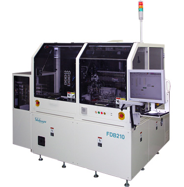
FDB210 / 211 (Thermo-compression (TC) bonding system)
This high-throughput and high-accuracy thermo-compression (TC) bonder is for optical module assembly such as laser diode bonding, sub-mount bonding and silicon photonics bonding.
Options are available for multiple chip bonding and other bonding methods.
FDB210 covers tray supply while FDB211 covers grip-ring supply.
Features
- High-accuracy bonding (3 σ = ±2µm)
- Capable of handling micro chips.
- The automatic calibration mechanism stabilizes accuracy by canceling positional changes which occur with time.
- The parametric sequence control enables programming control of the force, temperature and timings.
- The force feedback method achieves high-accuracy force control.
- A variety of optional settings, such as eutectic bonding, correspond to various bonding methods easily.
Options
- Tool head
- N2 purge
- Dispenser
- Paste transfer unit
- Multi-chips support
- Gel pack support
- Ultra-low bonding force head (min. 0.1 N)
Specifications
- Model
- FDB210 / 211
- Applicable product type
- VCSEL/LD (Laser Diode)/PD (Photo Diode)/Optical module/Analog device/LED/etc
- Substrate size
- 0.5 mm square to 10.0 mm square
- Chip size
- 0.25 mm square to 5.0 mm square
- Chip supply method
- FDB211: grip ring (FDB210: tray supply)
- Chip heating method
- Pulse heating
- Substrate heating method
- Pulse heating
- Bonding load
- 0.2 to 8.8 N
- Mounting accuracy
- ±2µm (3 σ)
- Unit dimensions
- 1730 (W) X 1981 (D) X 1650 (H) mm
- Unit weight
- 3500 kg
- INQUIRES
-
SHIBUYA CORPORATION
Mechatronics Div. S&H Div. Semi-Conductor System Sales Dept.
2-232, Wakamiya, Kanazawa 920-0054
TEL +81(76)262-2201 FAX +81(76)262-2210
E-mail sh-info@shibuya.co.jp