

SEMICONDUCTOR / BATTERY MANUFACTURING SYSTEMS
FDB210P High-Accuracy Bonder for Optical Communication and Optical DevicesUltra-high accuracy bonder / Accuracy: ±0.8µm
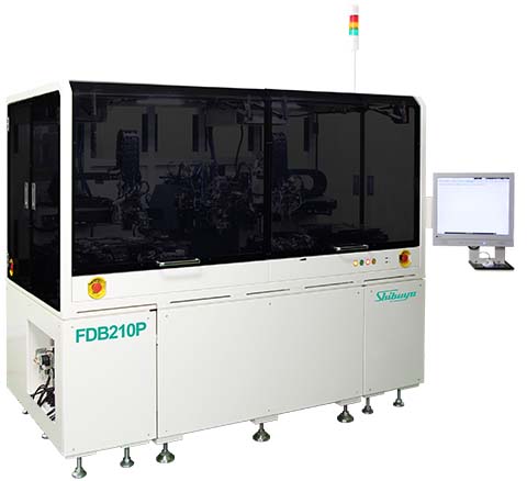
FDB210P (Thermo-compression (TC) bonding system)
This is ultra-high precision thermo-compression (TC) bonder for optical module assembly.
The high-accuracy alignment mechanism ensures ±0.8µm (3 σ).
Features
- Ultra-high accuracy bonding (3 σ = ±0.8µm)
- The small foot-print saves machine set-up space.
- Capable of handling micro chips.
- The automatic calibration mechanism stabilizes accuracy by canceling positional changes which occur with time.
- The parametric sequence control enables programming control of the force, temperature and timings.
- The load feedback method achieves high-accuracy load control.
- Unique N2 purge mechanism controls oxygen concentration lower than 100ppm.
Specifications
- Model
- FDB210P
- Applicable product type
- VCSEL/LD (Laser Diode)/PD (Photo Diode)/Optical module/LIDAR/etc
- Substrate size
- 0.4 mm square to 10.0 mm square
- Chip size
- 0.25 mm square to 6.0 mm square
- Chip supply method
- Tray supply、Glip ring
- Chip heating method
- Pulse heating(Max.450°C)
- Substrate heating method
- Pulse heating(Max.450°C)
- Bonding load
- 0.1 to 5 N
- Mounting accuracy
- ±0.8µm (3 σ)
- Unit dimensions
- 2000 (W) X 1400 (D) X 1700 (H) mm
- Unit weight
- 2500 kg (machine only)
- INQUIRES
-
SHIBUYA CORPORATION
Mechatronics Div. S&H Div. Semi-Conductor System Sales Dept.
2-232, Wakamiya, Kanazawa 920-0054
TEL +81(76)262-2201 FAX +81(76)262-2210
E-mail sh-info@shibuya.co.jp