

SEMICONDUCTOR / BATTERY MANUFACTURING SYSTEMS
FUB281 High-Accuracy Bonder for Optical Communication and Optical DevicesHigh-accuracy & high-throughput bonder / Wide-variety bonding / Populated substrates / Laser diode / Accuracy of Face Up mode: ±3µm,
Face Down mode: ±2µm
FUB281 (Thermo-compression (TC) bonding system)
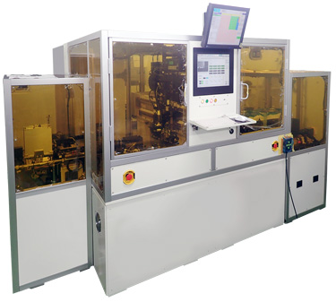
This high-throughput and high-accuracy thermo-compression (TC) bonder is for optical module assembly by handling aggregate substrates.
Available option enables a wide range of supply pattern and bonding methods.
Features
- High-accuracy bonding
Face Down mode (when the bonding plane is recognized): ±2µm (3 σ)
Face UP mode (when the top surface pattern is recognized): ±3µm (3 σ)
*Under high-accuracy mode - The automatic calibration mechanism stabilizes accuracy by canceling positional changes which occur with time.
- The dual stage configuration achieves high productivity by executing resin transfer and chip bonding simultaneously.
- Capable of handling micro chips.
- Supports supply of a large variety of products.
Options
- Tool head and various attachments
- Dispenser mechanism
- Resin transfer mechanism
- UV irradiation mechanism
Specifications
- Model
- FUB281
- Applicable product type
- VCSEL/LD (Laser Diode)/PD (Photo Diode)/Optical module/Analog device/LED/etc
- Substrate size
- Max. 100 × 150 mm
- Chip size
- 0.25 mm square to 5.0 mm square
- Chip supply method
- Grip ring / Gelpack tray
- Bonding load
- 0.05 to 5.0 N
- Mounting accuracy
- ±2µm (3 σ) for Face down mode
±3µm (3 σ) for Face Up mode - Unit dimensions
- 2840 (W) X 1940 (D) X 1700 (H) mm
- Unit weight
- 3000 kg
- INQUIRES
-
SHIBUYA CORPORATION
Mechatronics Div. S&H Div. Semi-Conductor System Sales Dept.
2-232, Wakamiya, Kanazawa 920-0054
TEL +81(76)262-2201 FAX +81(76)262-2210
E-mail sh-info@shibuya.co.jp