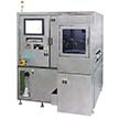
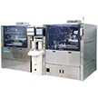
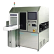
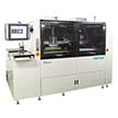
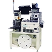
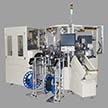
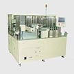
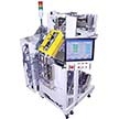
High-Accuracy Die Bonders
FUB281
High-accuracy & high-throughput bonder / Wide-variety bonding / Populated substrates / Laser diode / Accuracy of Face Up mode: ±3µm Face Down mode: ±2µm/
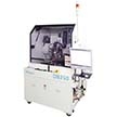
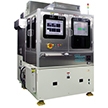
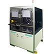
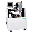
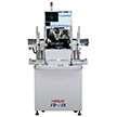
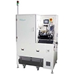
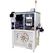
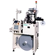
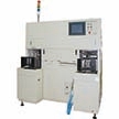
FUB281 (Thermo-compression (TC) bonding system)
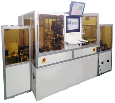
This high-throughput and high-accuracy thermo-compression (TC) bonder is for optical module assembly by handling aggregate substrates. Available option enables a wide range of supply pattern and bonding methods.
Features
- High-accuracy bonding
Face Down mode (when the bonding plane is recognized): ±2µm (3 σ)
Face UP mode (when the top surface pattern is recognized): ±3µm (3 σ)
*Under high-accuracy mode - The automatic calibration mechanism stabilizes accuracy by canceling positional changes which occur with time.
- The dual stage configuration achieves high productivity by executing resin transfer and chip bonding simultaneously.
- Capable of handling micro chips.
- Supports supply of a large variety of products.
Calibration
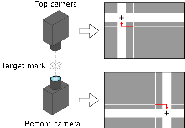
The calibration mechanism stabilizes alignment accuracy by detecting the relative positional deviation of the camera used for vision system alignment and feeding back the deviation when alignment for mounting is performed.
With vision system alignment, position accuracy cannot be maintained if the camera position changes because this results in changes in mounting positions as well. The camera is fixed in place and may not seem to be moving, but factors such as use of heating mechanisms and changes in ambient temperature cause the machine to expand/contract, resulting in changes in the camera position over time.
The calibration mechanism therefore offsets such positional changes that occur over time to stabilize alignment accuracy.
This mechanism first performs pattern matching using both the top camera and bottom camera with respect to the same target mark to detect each camera’s deviation from the target mark. By feeding back this deviation when alignment for mounting is performed, the deviation of the camera position is offset.
Options
- Tool head and various attachments
- Dispenser mechanism
- Resin transfer mechanism
- UV irradiation mechanism
Specifications
| Model | FUB281 |
|---|---|
| Applicable product type | VCSEL/LD (Laser Diode)/PD (Photo Diode)/Optical module/Analog device/LED/etc |
| Substrate size | Max. 100 × 150 mm |
| Chip size | 0.25 mm square to 5.0 mm square |
| Chip supply method | Grip ring / Gelpack tray |
| Bonding load | 0.05 to 5.0 N |
| Mounting accuracy | ±2µm (3 σ) for Face down mode ±3µm (3 σ) for Face Up mode |
| Unit dimensions | 2840 (W) X 1940 (D) X 1700 (H) mm |
| Unit weight | 3000 kg |
2-232, Wakamiya, Kanazawa 920-0054 JAPAN Telephone : +81(76)262-2201 Fax : +81(76)262-2210
Insights
Our ongoing commitment to pioneering the future of technology.